Fast Technology reported on May 10th that NVIDIA’s Blackwell series of artificial intelligence GPUs have just begun shipping, but its next-generation architecture is already emerging.
According to reports, the codename for NVIDIA’s new architecture is “Rubin,” named after the American astronomer Vera Rubin. It is expected to achieve a groundbreaking leap in performance while focusing on reducing power consumption to meet the expanding demands of future computing centers.
Analyst Ming-Chi Kuo revealed that the first AI GPU based on the “Rubin” architecture, the R100, is expected to enter mass production in the fourth quarter of 2025.
This also implies that the R100 may debut earlier for evaluation by customers, with shipments possibly starting in early 2026.
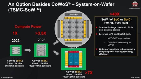
The R100 is expected to utilize TSMC’s 3-nanometer EUV FinFET process, featuring a fourfold lithography design compared to the current Blackwell B100 and continuing to utilize TSMC’s CoWoS-L packaging technology.
Furthermore, the R100 is poised to be one of the first chips to adopt HBM4 stacked memory, with an expected 8 stacks, although the exact stack height remains unspecified.
Simultaneously, the Grace Ruben GR200 CPU+GPU combination may feature a brand-new “Grace” CPU manufactured on the 3-nanometer node and may employ optical shrink technology to further reduce power consumption.