Tianjin University Team Successfully Creates World’s First Graphene Semiconductor
On January 4th, a report from the official website of Tianjin University revealed a breakthrough by the team led by Marei at the International Research Center for Nanoparticles and Nanosystems. Their research overcame a long-standing technical challenge that has hindered the development of graphene electronics. By precisely controlling the growth process of epitaxial graphene, they have successfully introduced a bandgap into the material, producing a novel type of stable graphene semiconductor. Their research paper, titled “Ultra-high mobility semiconductor epitaxial graphene grown on silicon carbide,” was published on the Nature journal website on January 3, 2024.
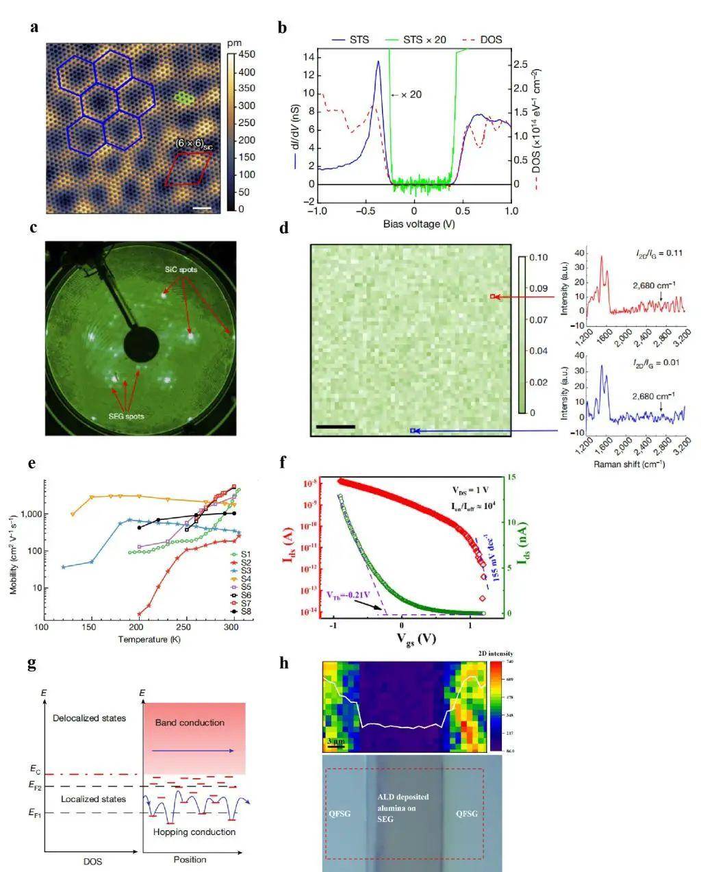
Image source: Tianjin University official website
Graphene, known as the first stable two-dimensional material at room temperature, possesses broad optical responsiveness, high charge carrier mobility, and high thermal conductivity. It’s deemed an ideal material for manufacturing smaller, more energy-efficient electronic components with faster transmission speeds. However, graphene’s unique Dirac cone energy band structure results in a “zero bandgap” characteristic, meaning a bandgap width of zero that cannot be effectively turned on and off under an electric field, limiting its application and development in the semiconductor field. This “zero bandgap” property has been a perplexing problem for graphene researchers for decades.
The Marei team employed an innovative quasi-equilibrium annealing method, rigorously controlling the growth environment’s temperature, timing, and gas flow to produce large, monolayer, single-crystal domains of semiconductor epitaxial graphene (SEG). This graphene is epitaxially grown on silicon carbide wafers, allowing it to form chemical bonds with the silicon carbide, thus exhibiting semiconductor properties.
The research paper reveals that this graphene semiconductor has a bandgap of 0.6 eV and an electron mobility exceeding 5000 cm² V⁻¹ S⁻¹ at room temperature, displaying performance ten times greater than silicon. This means electrons can move with much lower resistance, which translates to faster computing capabilities in electronics, surpassing all current two-dimensional crystals by at least an order of magnitude. It is currently the only two-dimensional semiconductor with all the necessary properties for nanoelectronics.
Additionally, this graphene semiconductor boasts large growth areas, high uniformity, and a simple, low-cost production process, overcoming deficits of traditional production methods. The switch ratio of the field-effect transistors made from this semiconductor epitaxial graphene is up to 10⁴, meeting the current industrial application requirements.
Significantly, as the limits predicted by Moore’s Law draw near, this gapful semiconductor graphene offers a novel material choice for high-performance electronic devices. Its breakthrough properties fulfill the growing need for higher computing speeds and the miniaturization of integrated electronic devices. Not only does it pave a new path for high-performance electronic devices surpassing traditional silicon-based technologies, but it also injects new vitality into the entire semiconductor industry.
By Zhang Xinyi and Zhao Yutong (Intern reporters)
Edited by Qiu Jiangyong
Designed by Maria
Supervised by Lian Xiaodong