Intel Achieves Milestone with World’s First High Numerical Aperture Extreme Ultraviolet Lithography System
Recently, Intel’s newly established chip fabrication business announced the successful assembly of the world’s first commercial High Numerical Aperture Extreme Ultraviolet (EUV) lithography scanner, marking a significant milestone in the chip manufacturing industry.
The name might sound perplexing, but it’s touted as the most advanced semiconductor manufacturing equipment ever, paving the way for future generations of computer chips that are even more advanced and powerful than current processors.
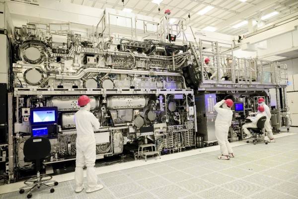
Intel revealed that the TWINSCAN EXE: 5000 High NA EUV tool was manufactured by ASML Holding NV, a chip manufacturing equipment company based in the Netherlands, and then assembled at Intel’s research facility in Hillsboro, Oregon, USA. Currently undergoing calibration at the facility, once completed, it will play a crucial role in advancing Intel Foundry’s future process roadmap. Intel states that this machine significantly enhances the resolution and feature expansion of next-generation chips by altering the optical design used to project printed images onto silicon wafers.
Next-Generation EUV
High Numerical Aperture EUV lithography is widely seen as the next generation of EUV lithography, a technology used in the semiconductor industry to manufacture integrated circuits. EUV lithography is a technique that relies on extreme ultraviolet light, which doesn’t naturally exist on Earth, to create intricate patterns on silicon wafers.
According to Intel, this extreme ultraviolet light is generated by powerful lasers heating tin droplets to nearly 220,000 degrees Celsius, a temperature almost 40 times higher than the average surface temperature of the Sun. The light reflects off a mask containing the desired circuit pattern and is then projected onto silicon wafers using optical systems with some of the most precise mirrors ever made, etching these circuits onto the silicon.
Numerical aperture is a metric that measures a machine’s ability to collect and focus light rays. This high NA EUV technology employs advanced optical designs to project patterns onto silicon wafers, leading to advancements in resolution and transistor size.
Intel’s Upcoming 14A Process
In February, Intel announced the spin-off of its fabrication business into an independent entity and detailed the upcoming Intel 14 manufacturing process.
The Intel TWINSCAN EXE: 5000 High NA EUV machine is roughly the size of a double-decker bus and reportedly costs $350 million. It arrived at Intel’s research center at the end of last year, and since then, Intel has been steadily assembling it. Now operational, it will be capable of producing transistors smaller than any existing lithography system, enabling Intel to realize its most advanced manufacturing processes.
Currently, the Intel 18A node is Intel’s most advanced manufacturing process, but it will be replaced by the Intel 14A process, expected to enter production in 2027.
The Intel 14A process will enable laser beams to carve transistors on silicon with a resolution of just 8 nanometers, a significant improvement over the 13.5-nanometer resolution of the Intel 18A process. Additionally, Intel states that this High NA EUV machine will reduce processor defects and increase chip production yields.
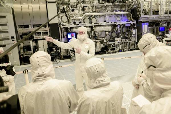
Mark Phillips, Intel Fellow and Director of Lithography, Hardware, and Solutions, said, “With the addition of High NA EUV, Intel will have the most comprehensive lithography toolset in the industry, enabling the advancement of future process capabilities beyond Intel 18A in the latter half of this century.”
Increasing Transistor Density
The more advanced Intel 14A process will lead to processors with greater functionality than existing ones, paving the way for significant advancements in AI and other emerging high-performance computing applications.
ASML has already demonstrated printing dense lines as small as 10 nanometers on silicon wafers in its research lab in Veldhoven, Netherlands, representing the finest lines ever printed on chips and helping validate the ambitions of the Intel 14A process.
Intel states that by using the Intel 14A process, it will be able to print on silicon wafers 1.7 times smaller than those manufactured by existing EUV machines, opening the door to 2D feature scaling and increasing density by 2.9 times, extending the assumption of Moore’s Law, which posits that the number of transistors on a chip doubles every two years. Additionally, High NA EUV supports higher imaging contrast, requiring less light per exposure and reducing the time required to print each layer, accelerating wafer output.
Intel states that the TWINSCAN EXE: 5000 system was shipped to the United States in 43 cargo containers, then packed into over 250 pallet boxes for transportation to the factory in Oregon. These containers were loaded onto multiple cargo planes bound for Seattle, then transferred to 20 trucks for the final leg of the journey.
More Advanced Machines on the Horizon
While Intel’s experts are busy calibrating the new machine, Intel is already planning similar logistics for the next suite— the TWINSCAN EXE: 5200B system, expected to further increase productivity, with the ability to etch over 200 wafers per hour.
However, Intel may not be the first to deploy the next generation of EUV machines. In December last year, New York, IBM, Micron, and several other organizations announced plans to establish an advanced semiconductor research lab in Albany, hosting similar systems.
These companies also plan to acquire a set of Twinscan EXE: 5200 systems, which will be used to realize the envisioned 2-nanometer chip manufacturing process, even more advanced than Intel 14A, though it’s unclear when it will enter production.